FACILITIES
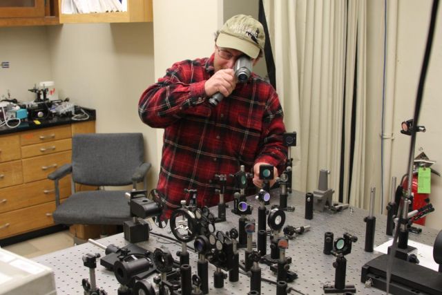
OPTICAL CHARACTERIZATION FACILITY
In the Optical Characterization Facility, light is used to probe the intrinsic properties of materials prepared by chemists and serves as an analytical and quality control tool. We study energy and charge migration in materials for novel optoelectronic devices, test new biosensors and materials for data storage, zap bacteria with laser beams, and provide state of the art technical capabilities that are not commonly available to non-expert chemists in their own laboratory. The optical characterization facility gives students the ability to have hands-on experience in modern optical spectroscopy. The facility manager assists its users in the design, assembly, and final analysis of experimental data. Custom optical experiments and support include photoconductive atomic force microscope, solar simulators for photovoltaics research or optical setups for characterization of organic semiconductors and many more chemical, materials and biological systems.
Contact Information
Facility Manager and Spectroscopist: Dr. Alexander Mikhailovsky
Location: Chemistry 3312
Phone: 805-893-2327
Email: mikhailovsky@chem.ucsb.edu
Webpage: Optical Characterization Facility
Major Capabilities and Areas of Expertise:
* Time-resolved fluorescence measurements in the range 50 ps – 10 s (time-correlated single-photon counting etc.).
* Transient absorption spectroscopy with sub-100 fs resolution
* Custom luminescence spectroscopy (temperature-dependence, photoluminescence up-conversion, thermoluminescnce, electroluminescence, quantum-yield measurements)
* Non-linear optical spectroscopy (multiphoton absorption and optical harmonics spectroscopy)
* Raman spectroscopy and microscopy
* High laser power processing of materials and Optical holography
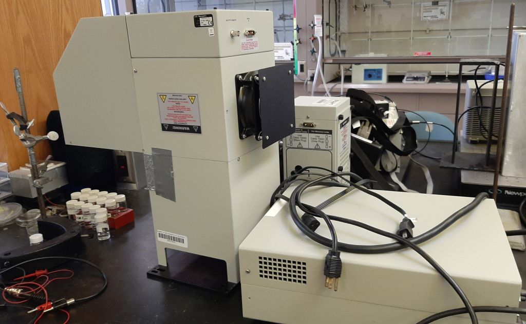
Facility Instrumentation include 1 kHz repetition rate, 100 fs pulse Ti:Sapphire amplifier, Ti:Sapphire femtosecond oscillator laser, optical harmonics generator, high power Ar-ion laser with single-mode operation capability, various smaller semiconductor and gas lasers. We also have several monochromators equipped with spectroscopic CCD cameras, single channel detectors and a high-end Raman microscope.
_______________________________________________
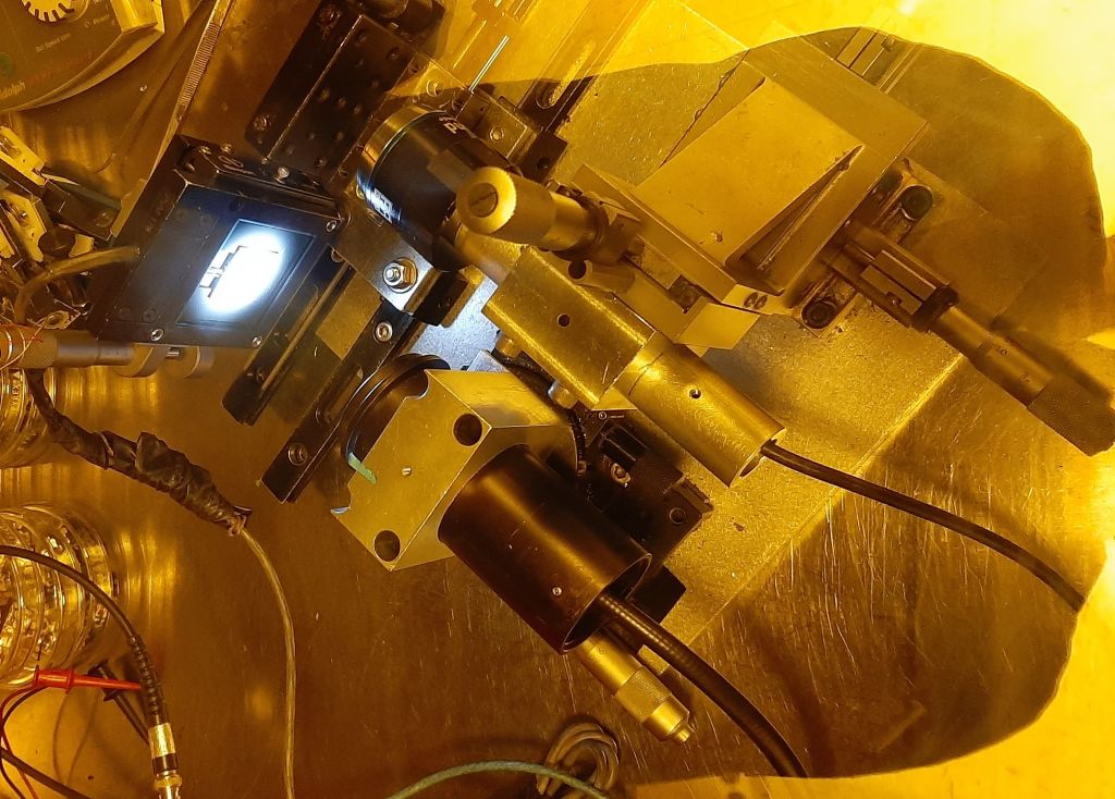
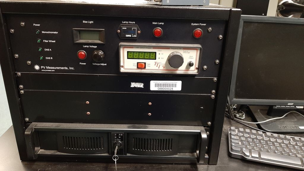
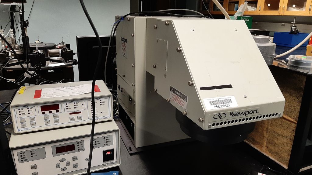
SOLAR SIMULATOR & EQE CHARACTERIZATIONS
- Setup 1 (CHEM 3142): Small illumination area, custom-built solar simulator, for testing samples inside a glovebox. Custom-built EQE setup with small beam-size, with characterization range from 300-1300 nm.
- Setup 2 (CHEM 3242): Newport 91192-1000 solar simulator (large area) and PV-measurement EQE characterization setup, with characterization range from 400-1450 nm
- Setup 3 (CHEM 3247): Newport 91150-1000 solar simulator (large area). Custom-built EQE setup with small beam-size, with characterization range from 300-1800 nm.
Facility Contact: Dr. Gaurab Thapa
Location: CHEM 3142, CHEM 3242, CHEM 3247
Email: gjthapa@ucsb.edu
 Setup 1
-
Setup 2
-
Setup 2
-
Setup 3
_______________________________________________
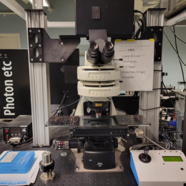
THE HYPERSPECTRAL IMAGING SETUP WITH COMBINED AND TEMPORAL RESOLUTION FOR IN-SITU MONITORING OF FILM OPTICAL PROPERTY
The hyperspectral microscope provides spectral and spatial information over very wide ranges in light wavelength. This also could maps photoluminescence, electroluminescence, fluorescence, reflectance, and transmittance.
Specification
Facility Contact : Ms. Hiba Wakidi
Location: Chemistry 4242
Email: hwakidi@ucsb.edu
- Spectral range: 400-1000 nm
- Spectral resolution (FWHM): < 2 nm
- Spectral channels: Continuously tunable
- Spatial resolution: Sub-micron - limited by the microscope objective NA
- Camera: CCD, EMCCD, sCMOS
- Excitation wavelengths: 532 nm
- Microscope: Upright or inverted, scientific grade
- White light illumination: Diascopic, episcopic, Hg, halogen
- Illumination options: Epifluorescence module, darkfield module (oil or dry)
Applications:
- Various Photovoltaic (Perovskite, CIGS, GaAs, Si and etc)
- Nano particles
- Biochemistry and Nanosensors
_______________________________________________
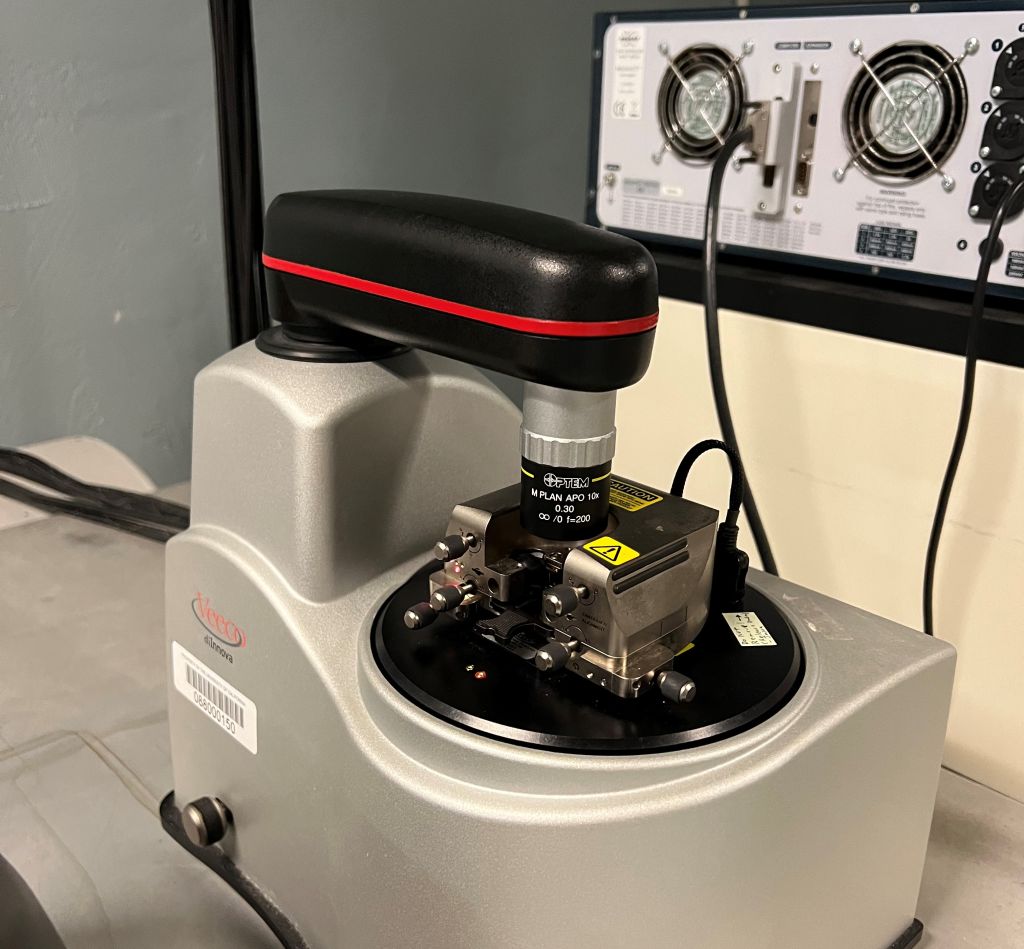
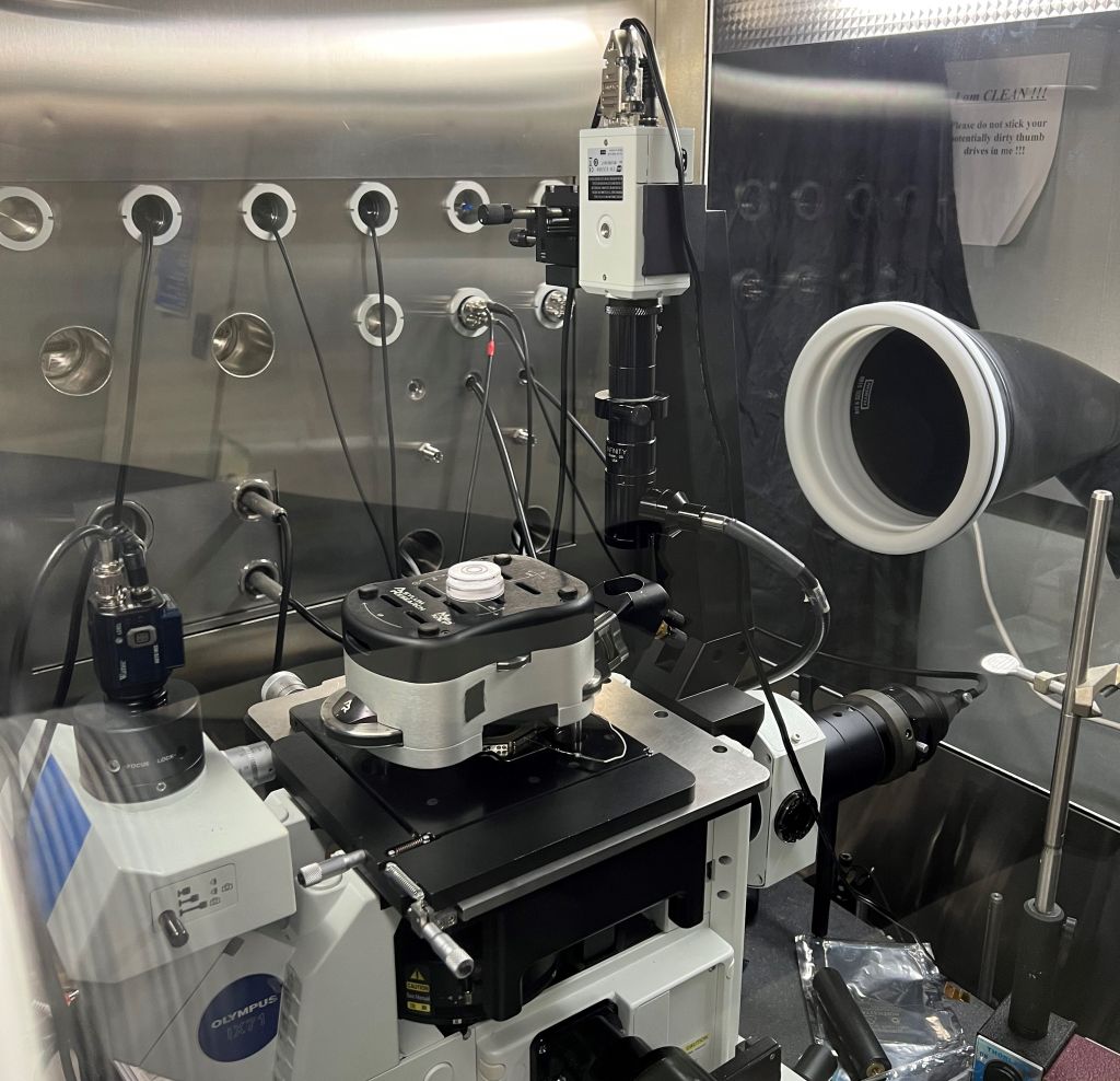
SCANNING PROBE MICROCOPES WITH MULTIMODES
- Atomic force microscopy (AFM) setup 1: Veeco Innova AFM on a hanging table. Imaging mode: non-contact, contact, c-AFM, EFM. Measurement in ambient air.
- Atomic force microscopy (AFM) setup 2: Bruker Multimode 8 on a hanging table.Imaging mode: non-contact, contact, c-AFM, EFM, Fluid-AFM, KPFM, STM. Measurement inside a glovebox.
- Atomic force microscopy (AFM) setup 3: Asylum MFP-3D mounted atop an Olympus inverted optical microscope. The setup is on a floating optical table. Imaging mode: non-contact, contact, c-AFM, photoconductive-AFM, EFM, Fluid-AFM, KPFM, STM. Measurement inside a glovebox.
Facility Contact : Ms. Hiba Wakidi
Location: Chemistry 3242
Email: hwakidi@ucsb.edu
-
Setup 1
-
Setup 2
-
Setup 3
_______________________________________________
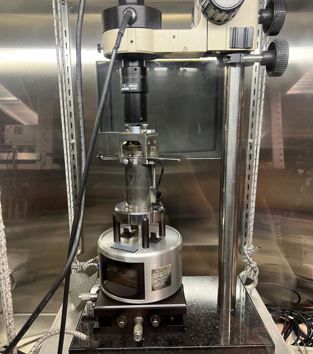
KELVIN PROBE
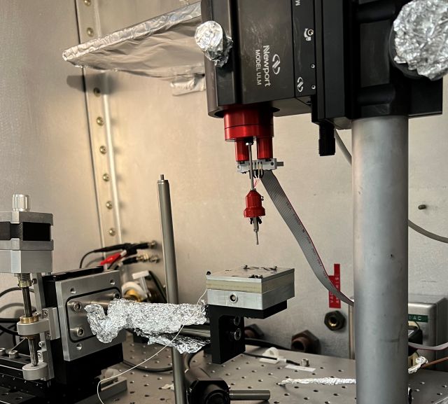
Scanning Kelvin Probe: KP Technology (Baikie) system inside a Faraday enclosure. Measurement of contact potential difference and work function with a resolution of 1-3 meV. Access to 2D and 3D work function plots of samples ranging from 50 mm to 350 mm. Measurement inside a glovebox.
Facility Contact : Ms. Hiba Wakidi
Location: Chemistry 3109
Email: hwakidi@ucsb.edu