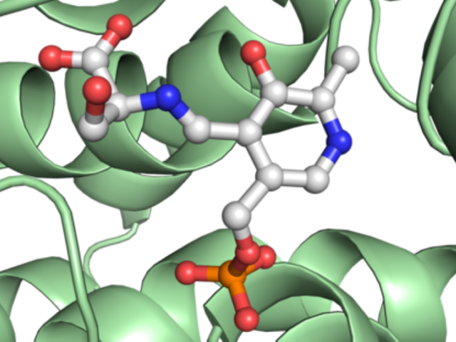
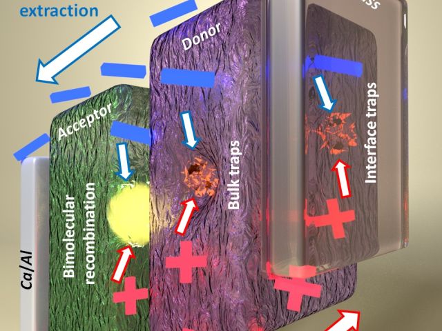
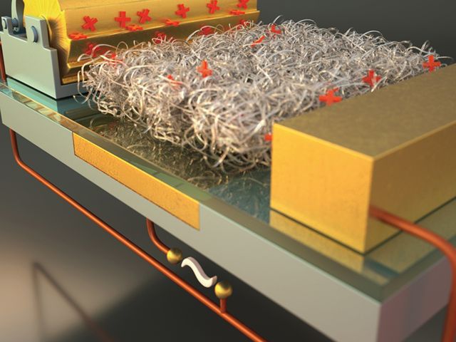
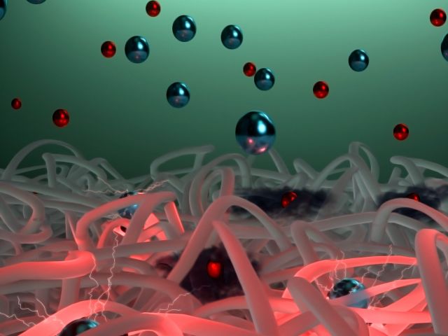
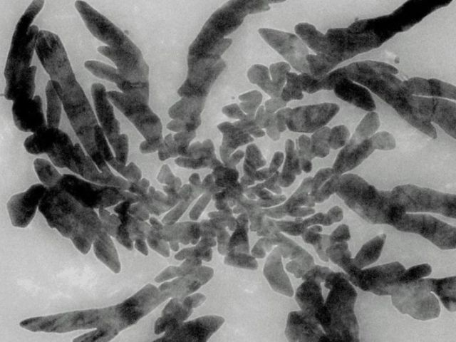
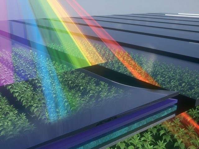
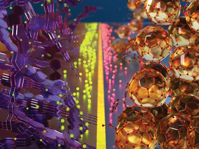
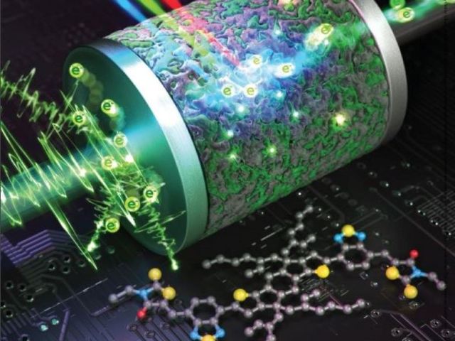
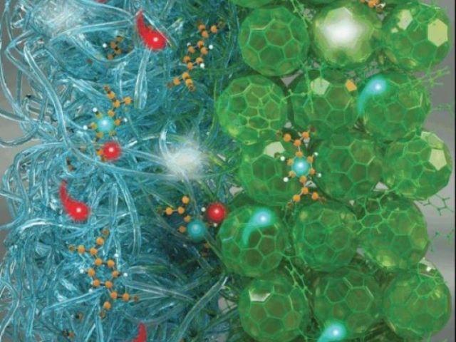
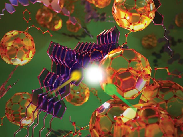
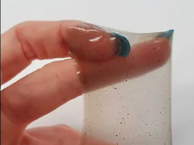
Our research touches several aspects of organic solar cells (OPVs): synthesis of new materials, nanoscale characterization, and device fabrication, engineering and optimization. With a dedicated team working on theory, simulation, and experiments, our ultimate goal is to understand how to achieve high efficiency photovoltaic devices.