"Vacancy-ordered double perovskite films formed via a two-step deposition process"
O. Kuklinski, A. Brumberg, and M. Chabinyc / Materials Department / University of California, Santa Barbara, 93106
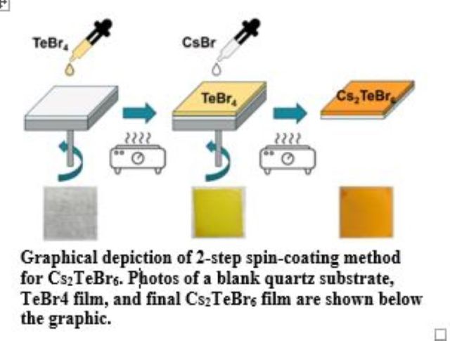
In this work, we report a new procedure for spin coating vacancy-ordered double perovskite Cs2TeBr6 films with high purity. Research interest in metal-halide perovskite semiconductors has recently skyrocketed due to their outstanding photophysical properties and solution-based processing methods, but growing films from solution frequently elicits the formation of defects that reduce their stability and performance.1. A two-step deposition method has been shown to suppress defect formation and is especially helpful for all-inorganic perovskites where precursors commonly have conflicting solubilities.2 The sequential spin coating of TeBr4 and CsBr produces uniform films with homogeneous grain size and high purity confirmed with scanning electron microscopy and X-ray diffraction, respectively. The conversion of precursors to final perovskite material is probed with Grazing-Incidence Wide Angle X-ray Scattering (GIWAXS). Ultraviolet photoelectron spectroscopy (UPS) experiments are carried out to determine the band energy levels for future device engineering. Lastly, the growth of mixed halide films is investigated by incorporating CsCl and CsI into the two-step deposition procedure. Diffuse reflectance spectroscopy and GIWAXS experiments reveal optical tuning through the selective formation of halide alloy phases.
References:
- He, C.; Liu, X. The Rise of Halide Perovskite Semiconductors. Light Sci Appl 2023, 12 (1), 15. https://doi.org/10.1038/s41377-022-01010-4.
- Han, Y.; Xie, H.; Lim, E. L.; Bi, D. Review of Two‐Step Method for Lead Halide Perovskite Solar Cells. Solar RRL 2022, 6 (6), 2101007. https://doi.org/10.1002/solr.202101007.